

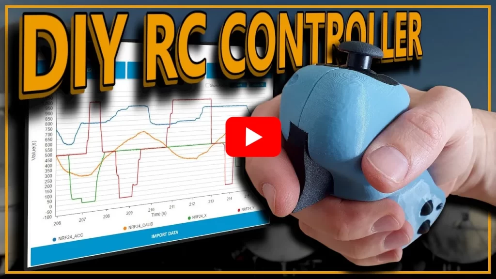
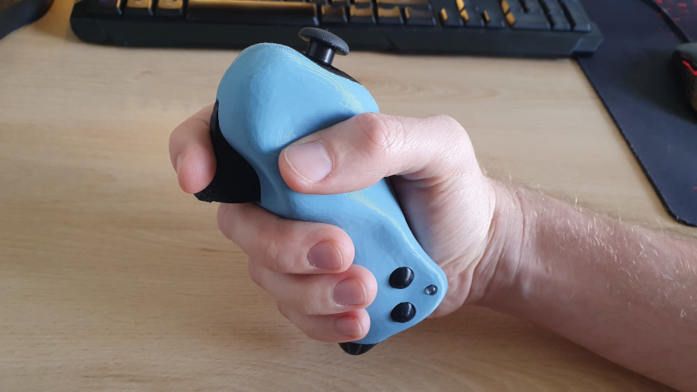
A radio controller can have a thousand applications. Usually, it’s a control of some vehicle, drone, or robotic manipulator. There are already a lot of DIY solutions on the Internet. However, this controller is different.
It’ll be the most comfortable RC Controller you’ve ever held. Because it will be perfectly suited to your unique hand 🙂
Introduction
This is the second part of this project. In the first one, we built this organic-looking enclosure. We modeled clay, which we later scanned using photogrammetry and then imported into Fusion 360. It is quite a complex topic, but very interesting. If you haven’t seen it yet: How to design an enclosure using photogrammetry?
Today, I’m going to show you how to modify the solid in Fusion 360 to fit all the components inside. Then, we’re gonna design and solder everything to the PCB. And finally, we’re gonna write software for STM32, which is the brain of this controller.
Let’s get started!
Video version
If you’d like to see a video summary of the whole process first, be my guest:
Source files
You can download all the source files such as Schematic, PCB layout, 3D model, BOM, and Firmware. If you want to receive all of them put the email below – I’ll send a link to you straight away.
Schematic
The main brain of this Transmitter is STM32L151C6. It’s a 32-bit microcontroller based on an ARM core. It has all the peripherals I need for this project, an easy-to-solder LQFP48 package.
If you’re not familiar with this family of microcontrollers yet, I really think it’s worth it.
Always when I’m planning a new embedded project, I start my search for a suitable microcontroller among the STM32. There’s an article on my website that describes step-by-step how to get started. If you’ve used an Arduino before, learning STM gonna be a piece of cake for you.
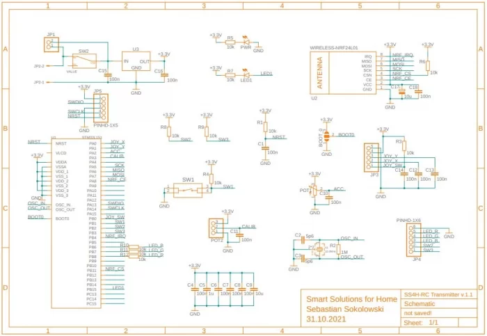
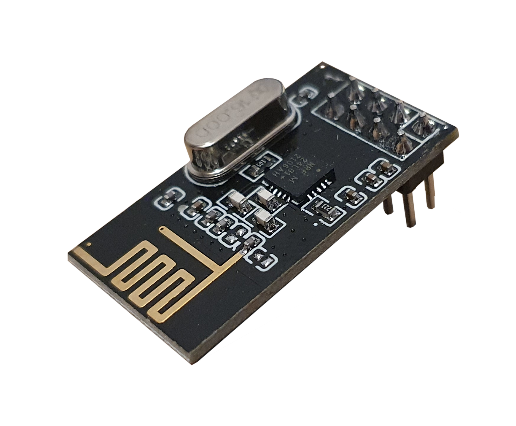
For radio communication, I probably used the most popular module: NRF24l01+ (Aliexpress). It’s loaded with features, it’s easy to use, costs less than 4 bucks, and there are tons of examples of how to use it on probably every platform available. What more could you ask for!
Additionally, there are four analog channels: two potentiometers (Aliexpress) and a thumb joystick (Aliexpress), two general-use buttons and RGB LED for feedback from the receiver e.g. communication status or battery level.
The rest of the schematic is standard for this kind of project. Some connectors, passive components, and low drop regulator (LDO).
Let’s move on to the design of the housing. Because the shape of the PCB depends on how much space can be created inside the case, we cannot do that right now.
3D Model
This part of the project was by far the longest one. At this point, it was very useful that in Fusion 360 electronics and mechanics are closely related. Thanks to this, I didn’t have to constantly switch between the PCB drawing program and the one for drawing the housing. In a design like this, the shape of the PCB, and the placement of components strictly depend on the housing. There’s no way to design a PCB first and then adjust the housing. It had to be done simultaneously.
I’m not gonna not bore you with a detailed description of how I model this solid. You would die of boredom! 🙂 Besides, if you created a model to fit your hand, the process would be a little different than mine anyway. Therefore, I’m just going to tell you how I started and then show you the end result. I’ll start where I left off in the previous article about photogrammetry.
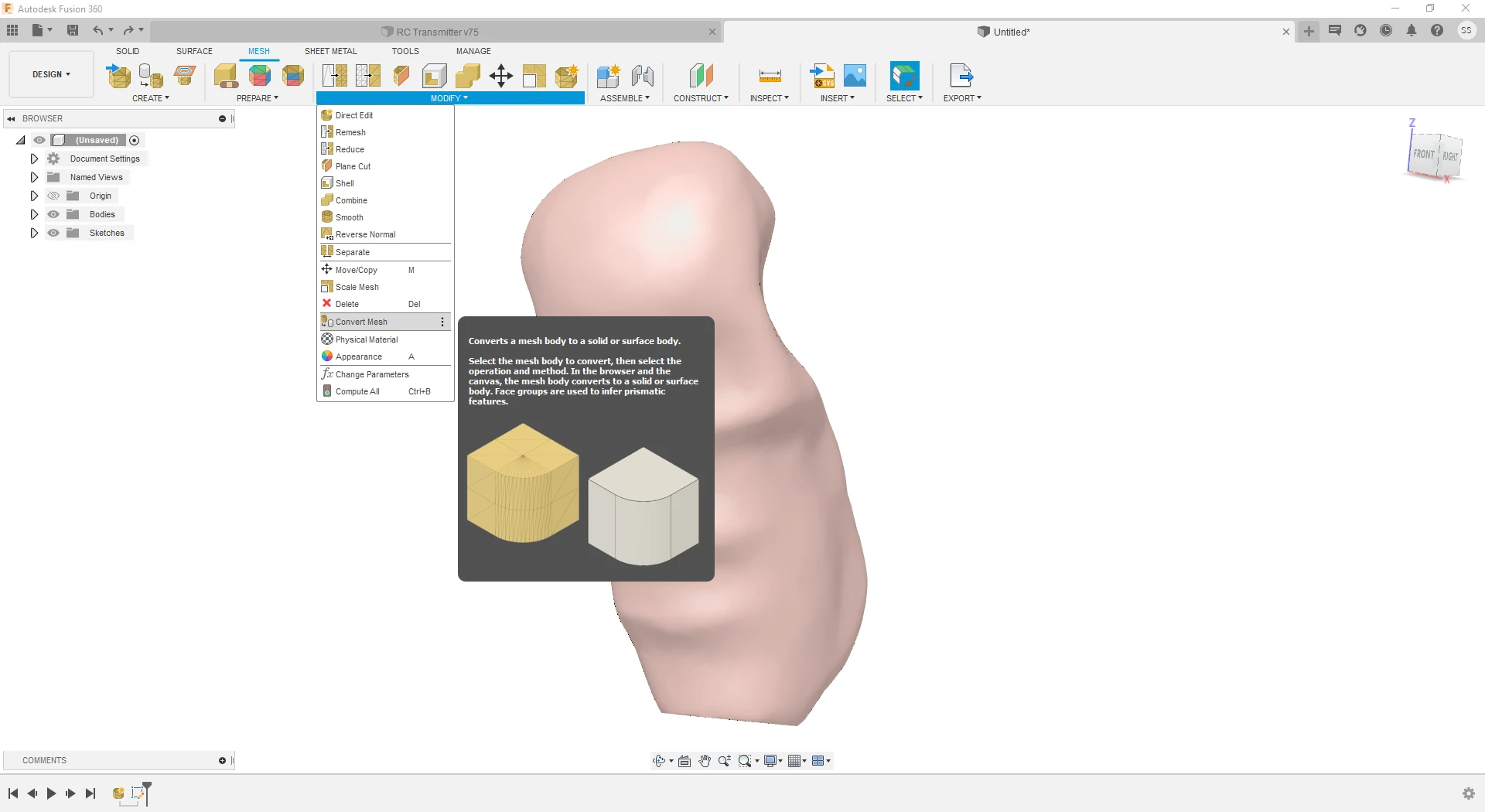
The first step is to transform a Mesh file into a solid. Luckily, it’s super simple in Fusion 360.
From the Modify menu, select Convert Mesh. And that’s it. You have a solid body ready for editing. And now the fun begins!
To make space for all the components, we need to make a hole inside the model.
It can be done in several ways, but I copied it, made it smaller, put it (more and less) in the middle. Then I split the body and removed the interior.
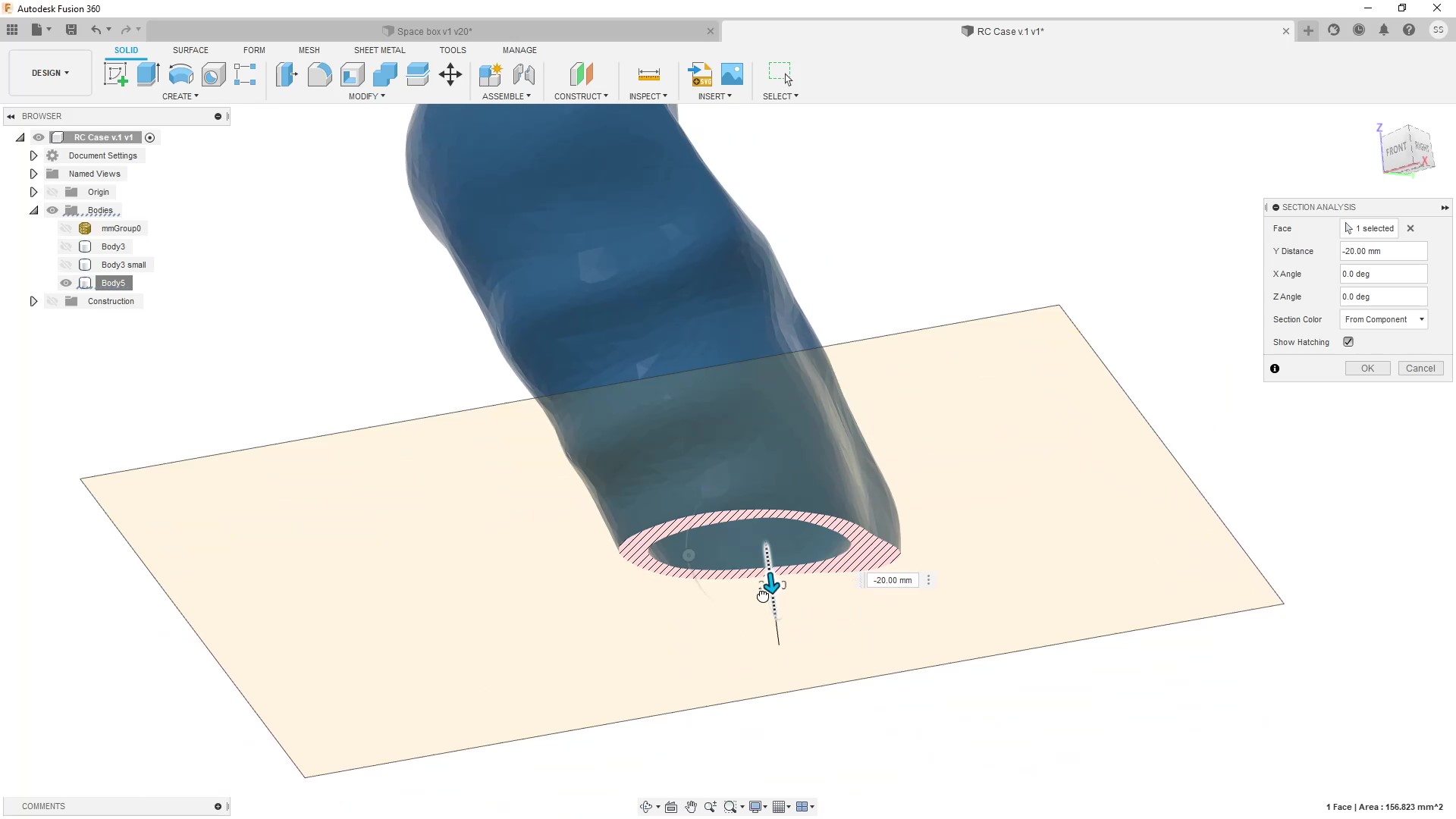
Maybe it’s not the most elegant way, but it’s fast and sufficient. You didn’t need the same wall thickness throughout the body. It’s only important so that the minimum value isn’t smaller than 0.86 mm. Which is the recommended value for a 0.4 mm nozzle size.

To make sure it’s ok, you can use the “section analysis” tool.
Then, we need to cut the model in half for easy access to the interior. Somehow we’re gonna have to pack all this electronic junk 🙂
Best to do this with the Plane and the Split Bode tool.

Now you should put all the components inside and prepare a place for them. It took me several hours. But maybe you can do it faster 🙂
Ultimately, the model looks like this:
PCB
As you may have noticed in the images above, the shape of the PCB we’ve defined in the previous step. So we just need to link this shape with the electronic design, and we can start drawing the PCB layout. To do this, select body of the PCB and then CREATE -> Create 3D PCB.
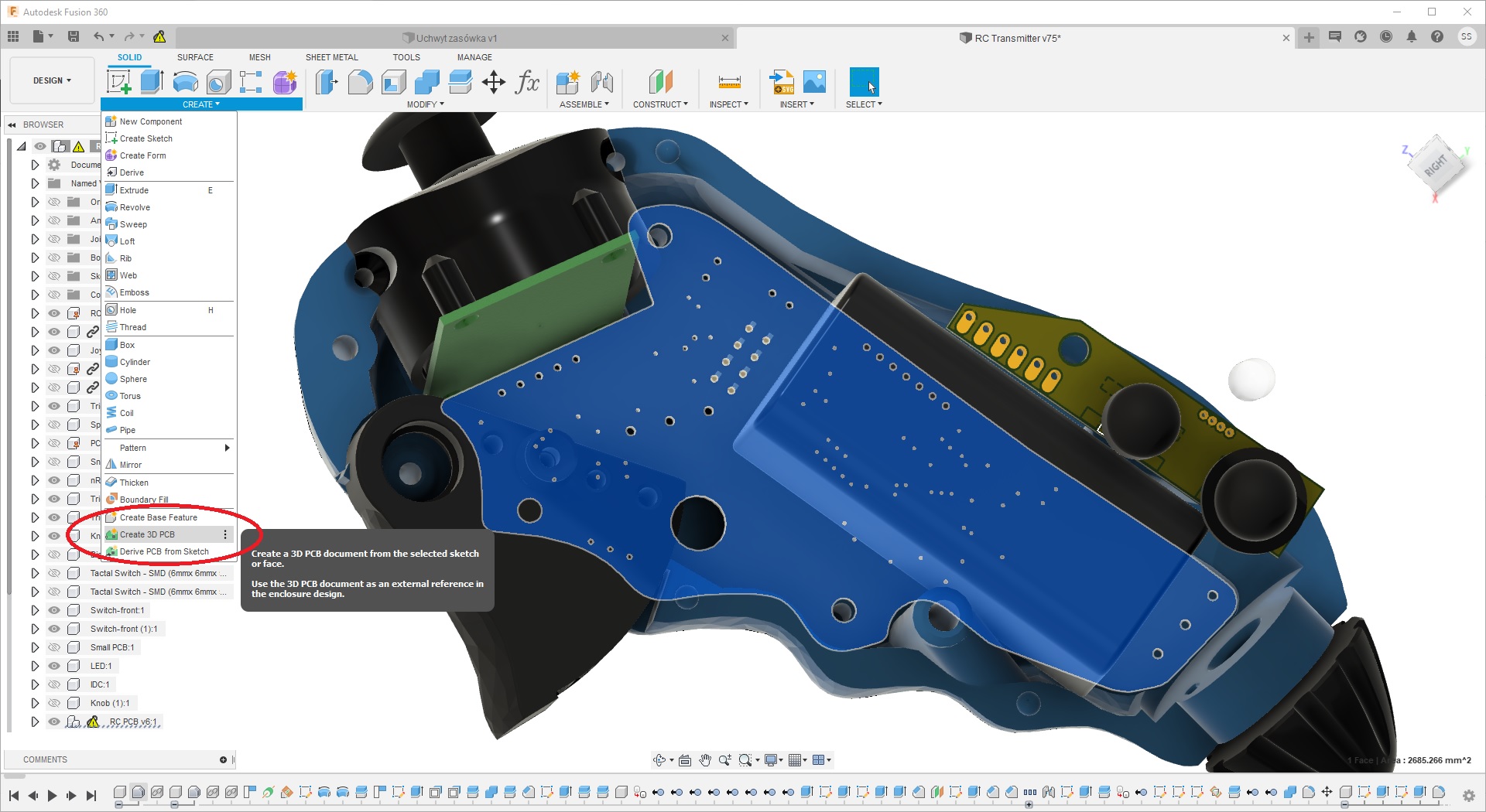
Then Link to 2D PCB, and select your previously created electronic design.

Now, all we need to do is draw the layout. But, it isn’t as easy as it may seem. For devices with so little space for components, everything has to be carefully thought out, especially for larger components such as capacitors, potentiometers, or the NRF24 module.
Since we’re talking about it, the NRF module isn’t placed in the best place. However, I couldn’t find a more suitable one. The housing has very limited space. This undoubtedly limited the range of the radio. But as it turned out, not as much as I was afraid. In tests, I found that communication is flawlessly up to 22 m (72 ft). You can see the entire test in my video.
The finished PCB looks like this:
Software
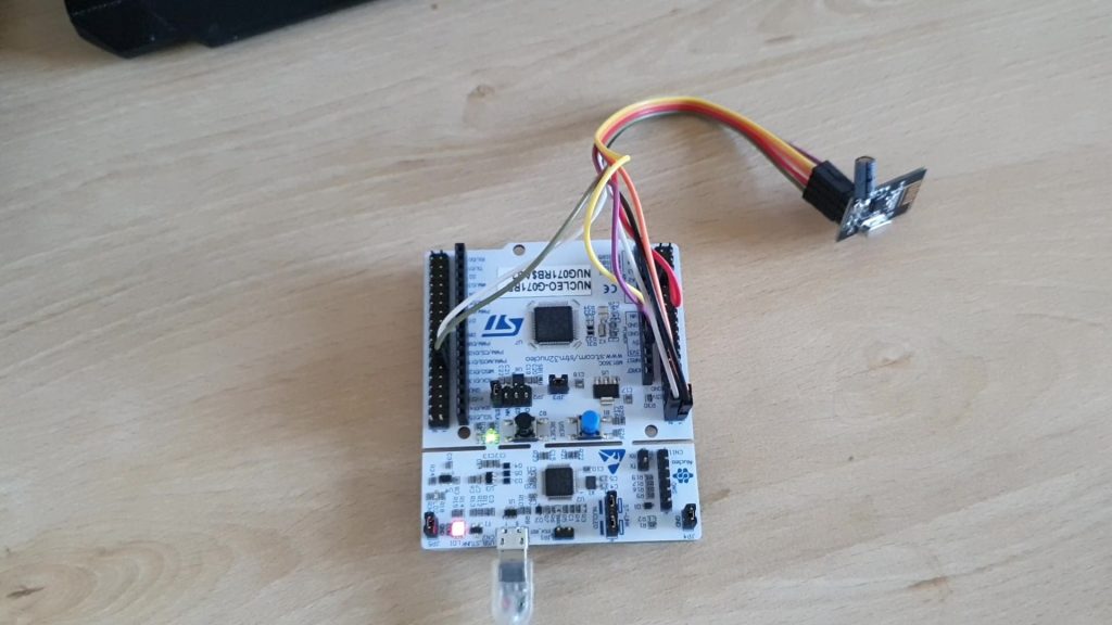
I wrote the whole project in STM32CubeIDE. It’s really powerful and completely free. That’s why it’s my default environment for the STM32 projects. To develop the radio communication, I had to make a temporary receiver with another NRF module. Luckily, I have a number of STM Nucleo evaluations boards littered in my workshop.
The code itself is pretty simple. Its only function is to send the current position of all analog and digital channels every 50 ms. What use will be made of this information is up to the Receiver. Currently, the Receiver doesn’t do anything useful. It just sends a confirmation that the data has arrived. But once the Receiver is the target vehicle, it will make good use of this data.
Of course, you can download the entire project and edit it freely. Bear in mind that you’re gonna need an external programmer. The cheapest ST-LINK V2 (like this: Aliexpress) will be ok.
Warning! Only for geeks! 🙂
Let’s dive a little deeper into the code:
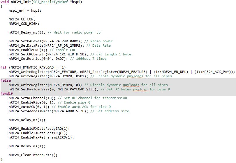
The NRF24 module can be both a Transmitter and a receiver. That’s why it has a common library. During initialization, you can configure which function the device should have. This is done with the void nRF24_Init(SPI_HandleTypeDef *hspi) function in the nRF24.c file
ADC measurement and data transfer from analog channels to the variables is done kind of automatically. I used DMA (Direct Memory Access) for this. Thanks to this, I don’t have to bother the processor every time the measurement is finished.
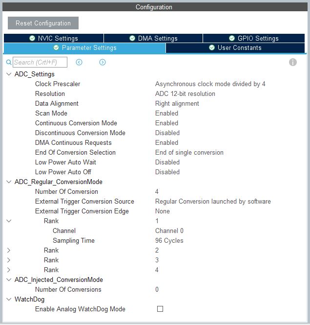
Measuring the ADC from Joystick and Calibration Potentiometer is simple. They are always connected to GND in the minimum position and to VCC in the maximum position. So always full ADC buffer (12 bit) is used.
In the case of Trigger, it’s not so easy.
It’s not possible to design the gears so that they always fit all potentiometers. To use its full range. And even so, it would make the assembly very difficult, because the small gear would’ve to be in the perfect position on the potentiometer spindle. Fortunately, there is a simpler solution 🙂
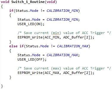
Trigger calibration
This model of microcontroller I chose has a built-in EEPROM memory! Which is not standard these days. Thanks to this, I can save what values the Trigger achieves physically in the min and max position. And then recalculate the current measurements to send the full range via the radio.
So, to calibrate it, put the JP1 jumper to power the microcontroller regardless of the trigger position. Press the SW1 button – green LED1 on the PCB will light up. Then press the trigger as far as it will go, and press the SW1 button again. LED1 will turn off. That’s it, the calibration is ready. You can pull out the jumper.
The functions that handle this calibration routine you can find in the buttons.c file.
In the main loop, all I do is check the state of the flag. It is set by the timer every 50 ms.
After entering this function, I first normalized the data from the ADC. The trigger values are converted following what I wrote earlier. And the 12-bit raw data from the ADC is split into two 8-bit variables because it is easier to send them via NRF24 this way.
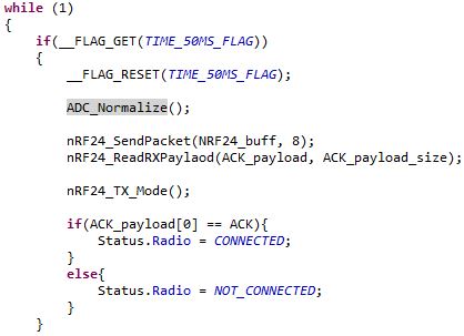
Then I send the data package to the receiver, and I’m waiting for an answer. If the answer appears, the communication in both directions was correct. And I can set radio status as a CONNECTED.
Assembly
In this chapter, I’m gonna show you how to assemble this particular transmitter. I mean, it will only be applicable if you create the exact same model (using my .stl and Gerber files) as me. If you use this article as a guide to making something your own, the assembly process will be different.
Nevertheless, there will probably be a lot of similarities anyway, so you’ll benefit anyway 🙂
Step 1
Start with soldering the pins in the Joystick module (Aliexpress) to the other side of the PCB. Then screw this module to the printed part of the Joy holder.
Step 2
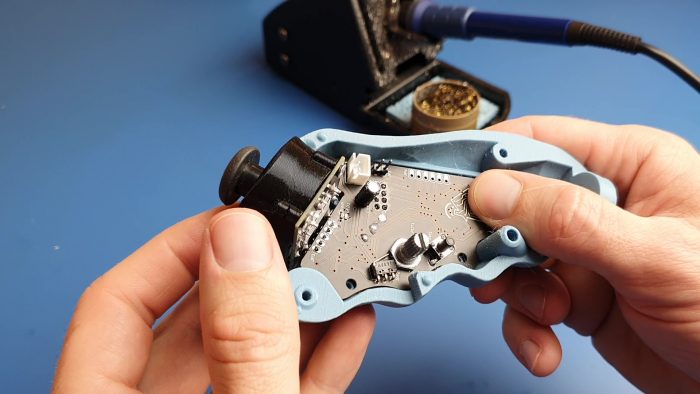
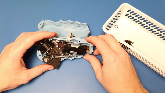
Place the module in the main Transmitter board, but don’t solder yet. First, put everything in the case and make sure the Joy holder fits snugly.
Step 3
Screw the PCB to the housing.

Step 4
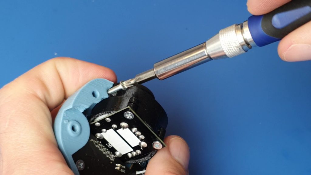
Tighten the two screws that secure the Joystick module and its holder. This will ensure that the housing and holder fit together well.
Step 5
Solder the joystick.
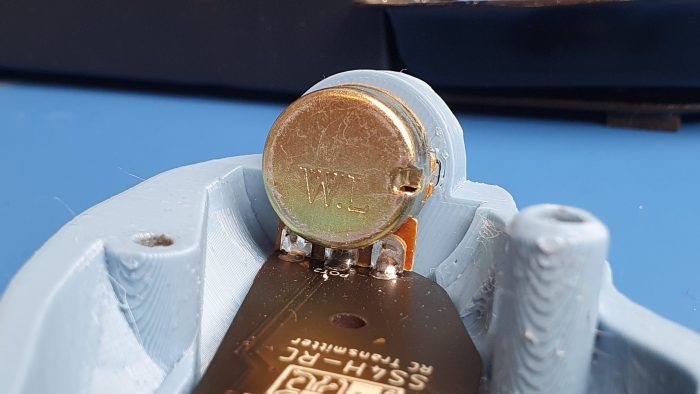
Step 6
To put the potentiometer in the hole on the back of the casing, you have to modify it. Cut the leads and use a file or Dremel to reduce the PCB a bit.
Then insert it into the mounting hole, secure with a nut and solder.
Step 7
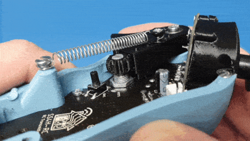
Install one end of the spring on the pillar.
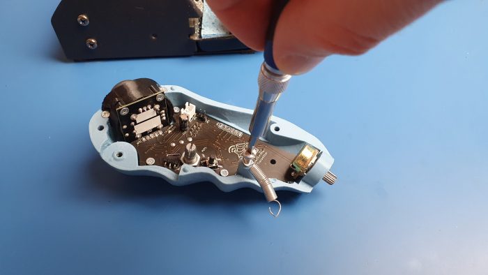
Step 8
Place the small gear on the axis of the potentiometer.
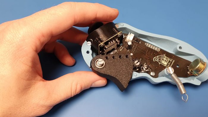
Step 9
Insert the two bearings into the Trigger part. Then screw it on.
Do it sensitively. If you do it too hard, the Trigger won’t turn. If you will do it for delicacy, it will be loose.
Make sure you can use the full range of the Trigger. If something is blocking it, it will probably be a gear that has reached its end. If so, turn the potentiometer a little.
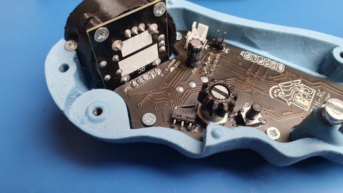
Step 10
Screw the Spring holder to the Trigger, and then use the pliers to install the spring.
As you can see, there are four holes where you can screw the Spring holder. Thanks to this, you can regulate how much force you need to use to press the Trigger.

Step 11
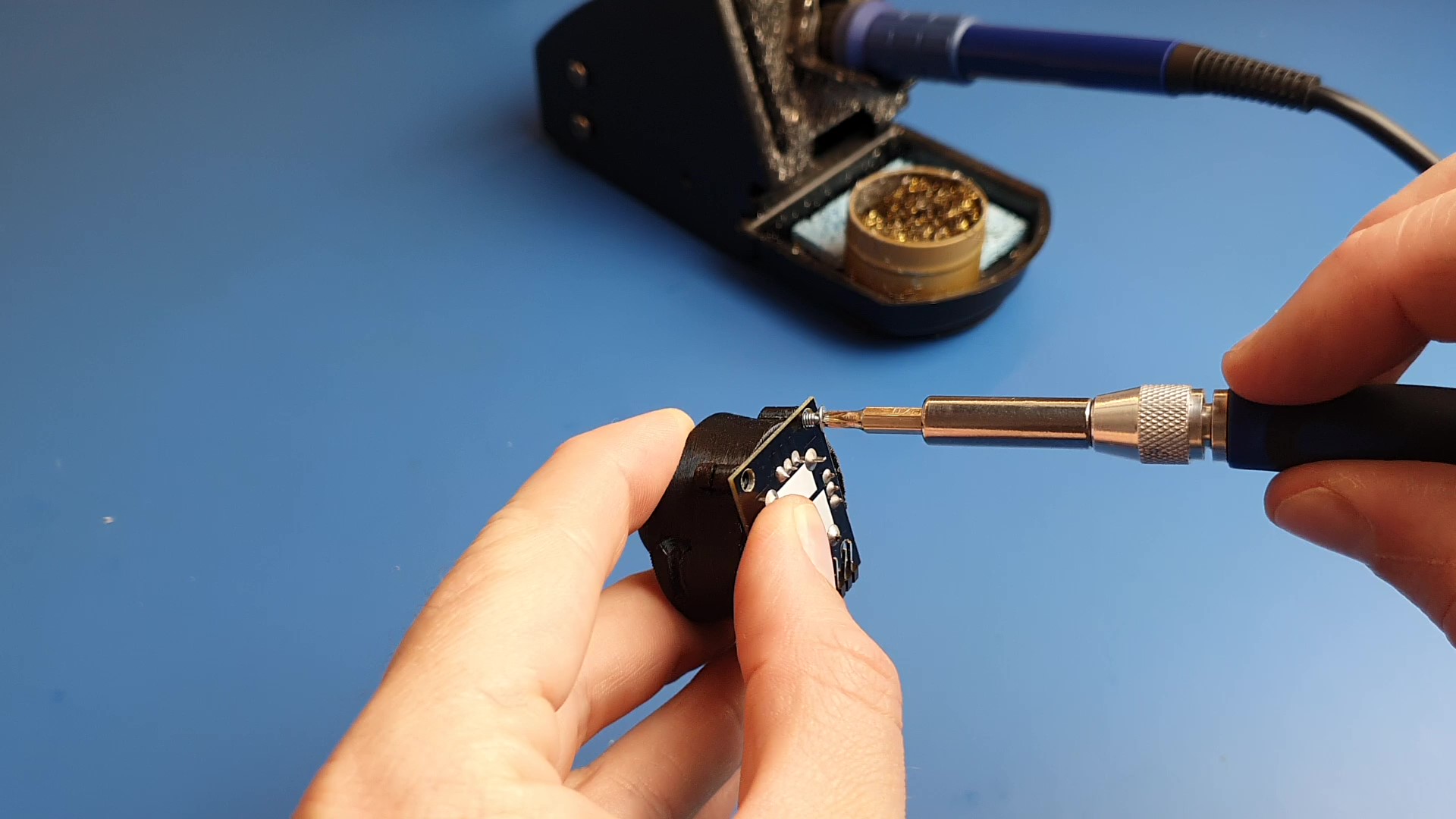
Mount the Interface board. It’s a PCB with two buttons and RGB LED. To make it easier, you can solder the IDC wires to the pads in advance.

Step 12
Using a soldering iron, plug the inserted nuts into both holes on the housing.
Step 13
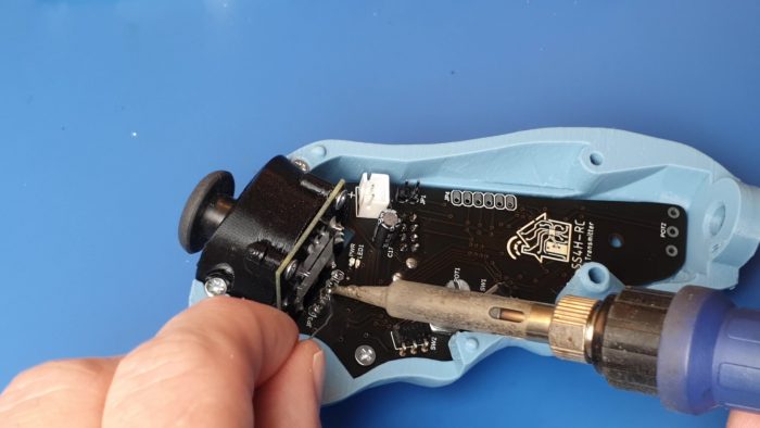
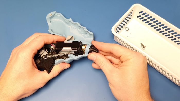
Solder the IDC wires to connect the Interface board to the Mainboard.

Step 14
Connect Battery pack to JP2 connector.
Step 15
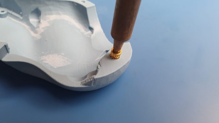
Install the knob on the rear potentiometer.
Step 16
Close both housing parts and screw them together.

That’s it! Your RC Controller is assembled and ready to use 🙂
Summary
Hope you found this article useful. I showed you a fairly large project broken down into small steps. Thanks to this, I hope you’re gonna be able to build something similar yourself.
If you’ve ideas for an upgrade or have any comments, feel free to write me an email: contact@smartsolutions4home.com
Related Articles
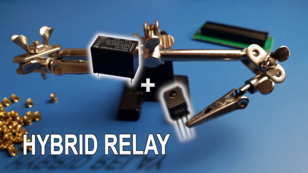
How Hybrid Relay works? – The Complete Illustrated Guide
The Hybrid Relay is a combination of electro-mechanical and semiconductor…
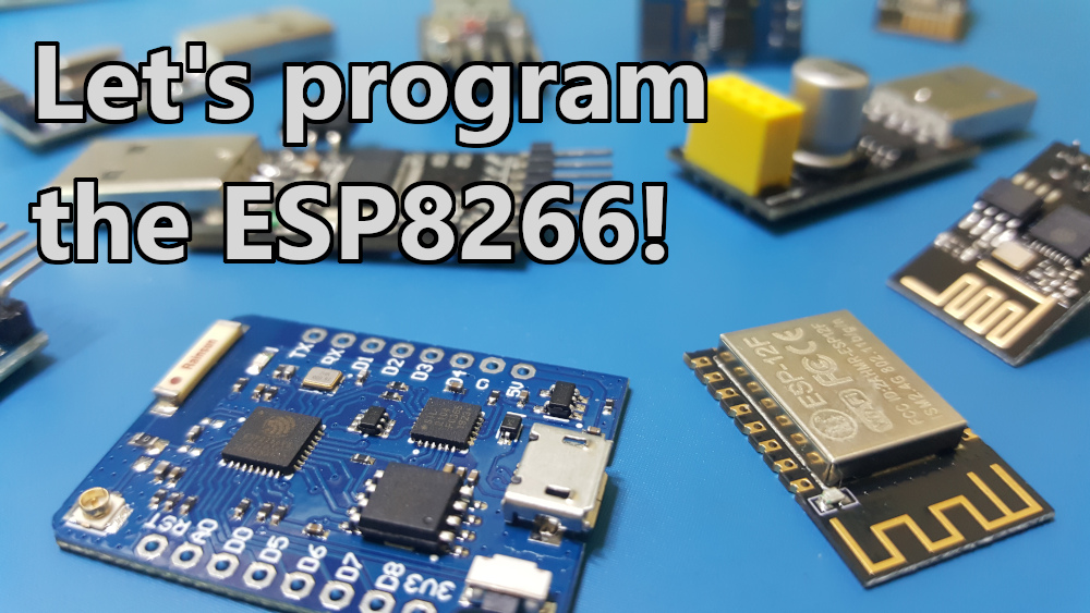
How to program an ESP8266 – With and Without Arduino
I discovered ESP8266 a few years ago. Since then, I’m…

How Smart Home save energy? – Real life examples
Do you want to reduce your bills by 30 –…